- 您现在的位置:买卖IC网 > Sheet目录2008 > MAX1434ECQ+D (Maxim Integrated Products)IC ADC 10BIT 50MSPS 100-TQFP
MAX1434
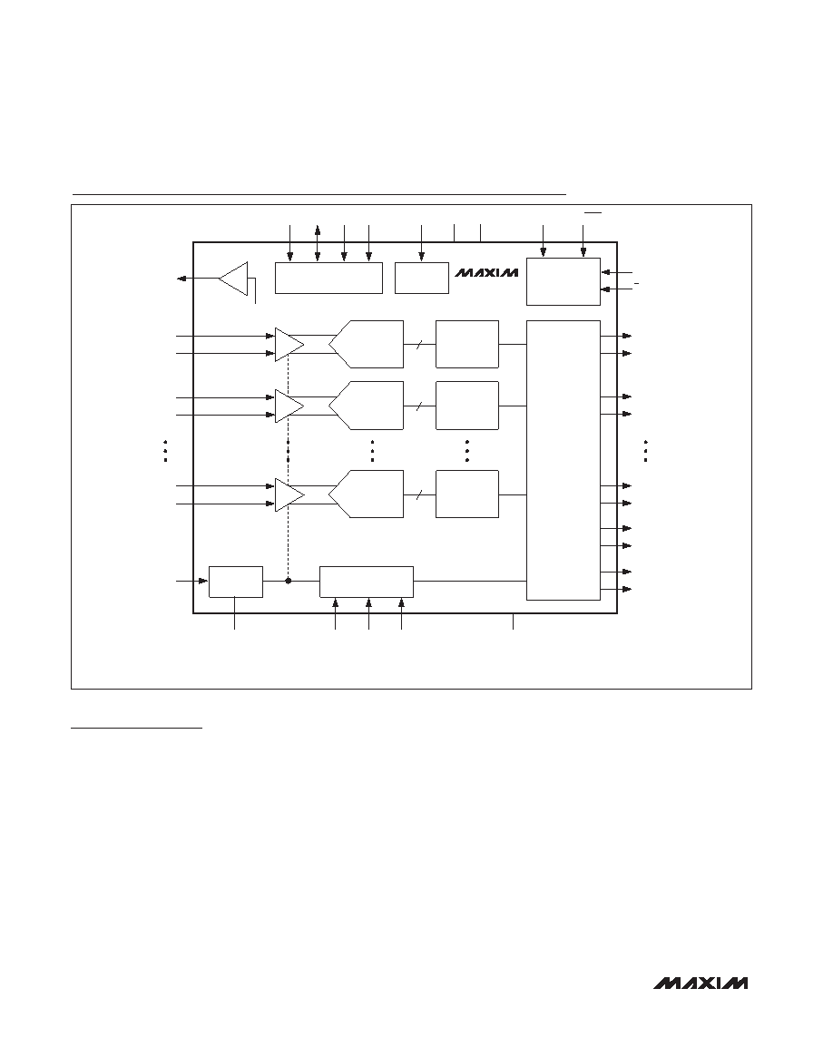
Detailed Description
The MAX1434 ADC features fully differential inputs, a
pipelined architecture, and digital error correction for
high-speed signal conversion. The ADC pipeline archi-
tecture moves the samples taken at the inputs through
the pipeline stages every half clock cycle. The convert-
ed digital results are serialized and sent through the
LVDS/SLVS output drivers. The total clock-cycle latency
from input to output is 6.5 clock cycles.
The MAX1434 offers eight separate fully differential chan-
nels with synchronized inputs and outputs. Configure the
outputs for binary or two’s complement with the T/B digital
input. Global power-down minimizes power consumption.
Input Circuit
Figure 1 displays a simplified diagram of the input T/H
circuits. In track mode, switches S1, S2a, S2b, S4a, S4b,
S5a, and S5b are closed. The fully differential circuits
sample the input signals onto the two capacitors (C2a
and C2b) through switches S4a and S4b. S2a and S2b
set the common mode for the operational transconduc-
tance amplifier (OTA), and open simultaneously with S1,
sampling the input waveform. Switches S4a, S4b, S5a,
and S5b are then opened before switches S3a and S3b
connect capacitors C1a and C1b to the output of the
amplifier and switch S4c is closed. The resulting differ-
ential voltages are held on capacitors C2a and C2b. The
amplifiers charge capacitors C1a and C1b to the same
values originally held on C2a and C2b. These values are
Octal, 10-Bit, 50Msps, 1.8V ADC
with Serial LVDS Outputs
12
______________________________________________________________________________________
LVDS/SLVS
OUTPUT
DRIVERS
PLL
5x
CLOCK
CIRCUITRY
REFERENCE SYSTEM
IN0P
IN0N
IN1P
IN1N
IN7P
IN7N
CLK
REFADJ REFIO REFP REFN
OUT0P
OUT0N
OUT1P
OUT1N
OUT7P
OUT7N
OVDD
AVDD
GND
CVDD
PLL3
PLL1
PLL2
LVDSTEST
DT
OUTPUT
CONTROL
MAX1434
T/H
10-BIT
PIPELINE
ADC
10:1
SERIALIZER
T/H
10-BIT
PIPELINE
ADC
10:1
SERIALIZER
FRAMEP
FRAMEN
CLKOUTP
CLKOUTN
T/H
10-BIT
PIPELINE
ADC
10:1
SERIALIZER
POWER
CONTROL
PD
SLVS/LVDS
T/B
*ICMV = INPUT COMMON-MODE VOLTAGE (INTERNALLY GENERATED).
CMOUT
ICMV*
Functional Diagram
发布紧急采购,3分钟左右您将得到回复。
相关PDF资料
MAX1444EHJ+T
IC ADC 10BIT 40MSPS 32-TQFP
MAX1499ECJ+
IC ADC 3 1/2DIG W/LED DVR 32TQFP
MAX152EPP+
IC ADC 8BIT 1UA PWR-DWN 20-DIP
MAX153EPP+
IC ADC 8BIT 1MSPS HI-SPD 20-DIP
MAX154AENG+
IC ADC 8BIT 4CH W/MUX&REF 24-DIP
MAX155AEPI+
IC ADC 8BIT 8CH T/H&REF 28-DIP
MAX157AEUA+
IC ADC 10BIT 108KSPS 2CH 8-UMAX
MAX160CPN+
IC ADC 8BIT UP COMPATIBLE 18-DIP
相关代理商/技术参数
MAX1434ECQ+TD
功能描述:模数转换器 - ADC 10-Bit 8Ch 50Msps 1.8V High Speed ADC RoHS:否 制造商:Texas Instruments 通道数量:2 结构:Sigma-Delta 转换速率:125 SPs to 8 KSPs 分辨率:24 bit 输入类型:Differential 信噪比:107 dB 接口类型:SPI 工作电源电压:1.7 V to 3.6 V, 2.7 V to 5.25 V 最大工作温度:+ 85 C 安装风格:SMD/SMT 封装 / 箱体:VQFN-32
MAX1434ECQ-D
功能描述:模数转换器 - ADC RoHS:否 制造商:Texas Instruments 通道数量:2 结构:Sigma-Delta 转换速率:125 SPs to 8 KSPs 分辨率:24 bit 输入类型:Differential 信噪比:107 dB 接口类型:SPI 工作电源电压:1.7 V to 3.6 V, 2.7 V to 5.25 V 最大工作温度:+ 85 C 安装风格:SMD/SMT 封装 / 箱体:VQFN-32
MAX1434ECQ-TD
功能描述:模数转换器 - ADC RoHS:否 制造商:Texas Instruments 通道数量:2 结构:Sigma-Delta 转换速率:125 SPs to 8 KSPs 分辨率:24 bit 输入类型:Differential 信噪比:107 dB 接口类型:SPI 工作电源电压:1.7 V to 3.6 V, 2.7 V to 5.25 V 最大工作温度:+ 85 C 安装风格:SMD/SMT 封装 / 箱体:VQFN-32
MAX1434EVKIT
功能描述:数据转换 IC 开发工具 Evaluation Kit for the MAX1434 MAX1436 MAX1437 MAX1438 RoHS:否 制造商:Texas Instruments 产品:Demonstration Kits 类型:ADC 工具用于评估:ADS130E08 接口类型:SPI 工作电源电压:- 6 V to + 6 V
MAX1436BECQ
制造商:Rochester Electronics LLC 功能描述: 制造商:Maxim Integrated Products 功能描述:
MAX1436BECQ+D
制造商:Maxim Integrated Products 功能描述:ADC OCTAL PIPELINED 40MSPS 12-BIT SERL - Rail/Tube
MAX1436BECQ+TD
制造商:Maxim Integrated Products 功能描述:OCTAL 12BIT 40MSPS ADC - Tape and Reel
MAX1436ECQ
制造商:Rochester Electronics LLC 功能描述: 制造商:Maxim Integrated Products 功能描述: